CASE STUDIES
Bonded Wafer and Metrology Defect Review System
The Situation
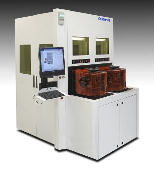
Olympus-ITA had developed a revolutionary confocal IR laser scanning microscopy technology for measuring bonded wafer parameters of 3D stacked ICs. The confocal capability of the microscope allows thin optical sectioning in Z and construction of 3D images of the bonded wafer interface and structures. This allows the user to characterize overlay alignment accuracy, perform thickness measurements, and image the bonded interface for defect analysis with a single instrument. To capitalize on their innovative technology, Olympus-ITA needed to rapidly integrate their technology in a 300mm fully automated platform.
The Challenge
As a technology innovator, Olympus-ITA wished to maintain their focus on delivering their unique technology to meet the customer’s critical needs. Developing a fully 300mm compliant automation platform is a complex undertaking that would have diverted critical resources. Olympus-ITA chose to partner with Owens Design as their development and manufacturing partner to provide a complete solution for their customers.
The Solution
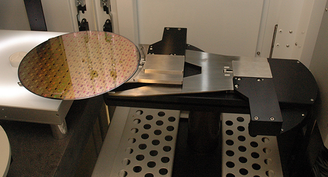
Owens Design worked closely with Olympus-ITA to understand their technology’s unique requirements. Then, drawing on a depth of experience in semiconductor automation, Owens Design developed a metrology platform that met Olympus-ITA’s precise needs. The solution included precision staging, vibration isolation, clean air flow, wafer handling robotics, load ports, and system framing. The wafer handling system incorporated an innovative design to accomodate severely warped wafers that are common with bonded pairs. The system fully met SEMI requirements for safety and factory automation.


