CASE STUDIES
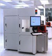
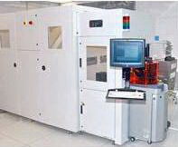
Atlas Metrology Automation Platform
Background
New opportunities for small startup metrology companies are being driven by next generation process and device technology. Namely smaller geometries, new materials and challenging integration issues require new technology solutions and new wafer characterization tools. However, transitioning the product from a bench top R&D lab tool into a fully capable process production tool is a difficult and time-consuming task. Tight market windows, limited resources and a core competency centered on metrology, not 300 mm factory capable tool development, compounds the problem.
To address this problem, Owens Design has developed a standard metrology automation platform that is designed to accommodate a variety of metrology process components. The use of a standardized tool platform drastically reduces overall tool development cost and time while also narrowing the scope of the internal development team to focus on only their core competencies.
Platform Description
The metrology tool platform uses a well-established industry standard 300 mm FOUP and/or 200 mm SMIF capable EFEM to reliably align and transfer wafers from the loadports to the inspection station. Overall airflow and pressure balance between the process stage and the EFEM has been optimized through CFD modeling to ensure clean wafer transfer.
When combined with the appropriate connectivity software, the platform will meet all 300 mm factory requirements. The design of the platform allows for wafer level thermal and vibration isolation at the inspection stage to ensure a controlled environment for tool-to-tool matching. A standard power distribution and control system with a GUI interface is also integrated into the system. The tool platform has been designed to meet Semi S2 (operator safety) and Semi S8 (operator ergonomics) requirements.
Metrology Integration
Owens Design will work closely with your team to integrate your specific wafer staging, metrology modules, optics, wafer alignment, and other components. Owens Design will customize the tool frame, skins, air flow, handling, and service access to meet your specific needs. Owens Design will also ensure the entire integrated tool meets all industry and regulatory standards.
Robust Automation Software
By way of our automation software partner, PEER Group, we offer an optional software application that executes all 300mm SEMI automation standards and has many fab-specific operational scenarios already built-in. Additional simulation testing results in trouble-free fab installation and fast customer acceptance. The PEER Tool Orchestrator™ (PTO) won the Semiconductor International Best Product award in 2007. Visit the PEER Group website to learn more about wafer transport robotics software.
SPECIFICATIONS
Wafer Sizes
- Wafer Sizes: 200 mm, 300 mm
- Substrate Types: Si, Quartz
Repeatability (measured at wafer hand-off location)
- Repeatability in X,Y,Z axis: 0.003 inches
- Repeatability in Theta axis: 0.1 degrees
System Throughput
- Total Throughput (excluding host tool process time): 150 wph
- Expected Time to First Wafer: 18 seconds
- Expected Swap Time (single end effector): 12 seconds
Cleanliness
- Front side: < 0.01 particles @ 0.1 µm, PWP
- Back side: < 1,500 particles @ 0.2 µm, PWP
- Mini-environment ISO Class 2 environment
Reliability
- MTBF > 10,000 hrs
- MTBS > 6-months
- Availability > 1000 hrs
- MTTR < 2 hrs
Interface / Facilities
- Wafer and Carrier Identification
- OCR (SEMI T7, M12 and M13 scribes)
- Carrier Auto ID
- UI: 15" Flat Panel Display, Trackball and Keyboard
- Facilities
- 110 VAC, 50/60 Hz, 8 amps
- 22 - 26 in Hg vacuum required
Regulatory Compliance
- Certifications (SEMI S2, S8 and CE Mark)
- SEMI E15.1, E44.1, E45, E46-95, E47.1, E57 E62, E63, E64, E84, E99
- I300I Integrated Mini-environment Design Best Practices
- I300I Factory Guideline, Version 4.1


