CASE STUDIES
Scaling E-Beam Based Tools into Semiconductor Fab-Ready System
Situation
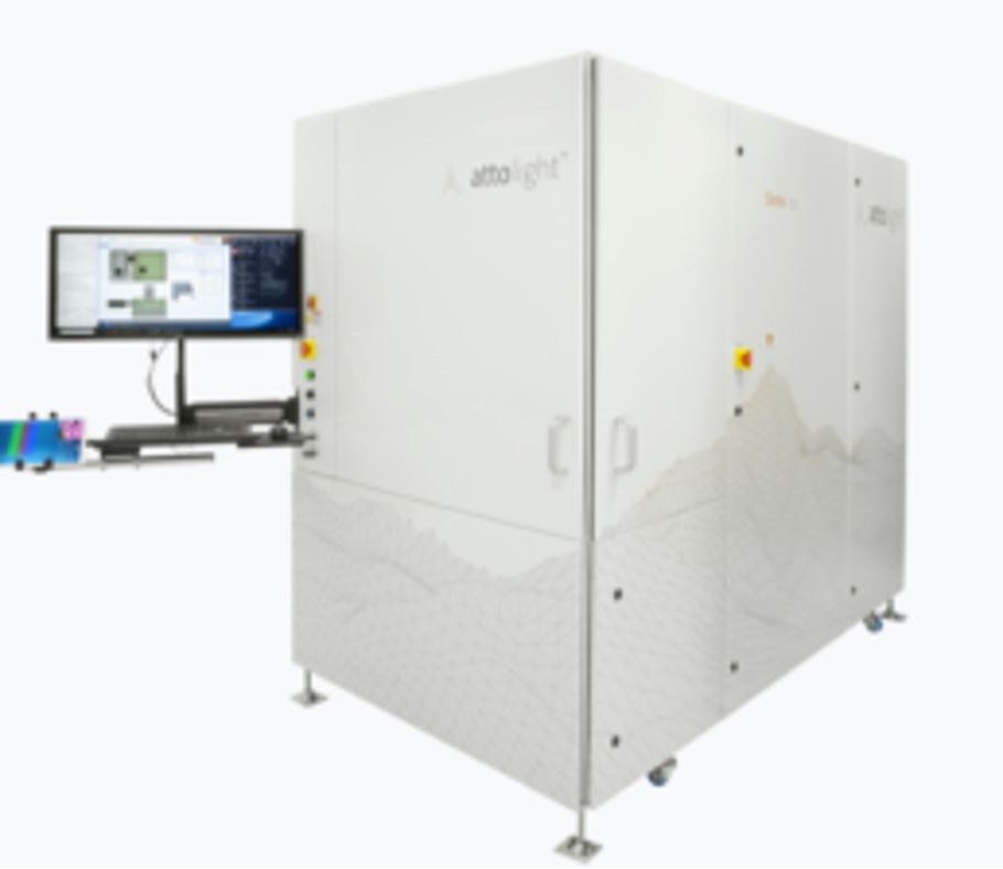
Attolight, a European startup metrology company, needed to rapidly scale their electron beam-based lab tool into a semiconductor fab-ready system to support their customer needs.
Problem
The startup lacked the tool development expertise and expert knowledge of semiconductor equipment standards to design and build a fab-ready tool. The e-beam tool required specialized knowledge of high vacuum, high precision e-beam compatible staging, vibration isolation, and semiconductor wafer handling. They were unable to find a single company to address all their requirements in Europe. Based on the prior experience of one of their chief business development officers, they reached out to Owens Design.
Solution
Owens Design designed and built a fab-ready system in record time. Owens developed a high vacuum system with an e-beam compatible stage that met the high positional accuracy and speed required to support the customer's use cases. They integrated an active isolation system to manage the high acceleration.
Owens provided a complete manufacturing infrastructure to support ongoing system manufacturing, including changes, configuration management, reliability, and cost reduction. “Owens Design was crucial in bringing our lab-based tool into the fab," said Attolight CEO, Samuel Sonderegger. "We have been very happy with the cooperation.” VP of Business Development, Sylvain Muckenhirn, added, “Within nine months, we had an industry-compatible product which was beautiful, wonderful, fast! Owens Design was like a second home to us.”
Attolight initially kept a demonstration tool at Owens Design’s Silicon Valley location to successfully support custom demonstrations.

