CASE STUDIES
Wafer Defect Review Module
The Situation
Macro defect inspection is one of the fastest growing segments in the wafer inspection industry. Macro defect inspection tools inspect the entire wafer surface for 0.5 micron and larger defects. Types of defects include pattern defects, incomplete etch, resist defects, scratches, and large scale contamination. Macro defect inspection is very versatile and can be used after CMP, litho, etch, and deposition. While the macro inspection method is very fast, it does not provide a high magnification image of the defect of interest later review and classification. This must be done using a defect review module.
The Challenge
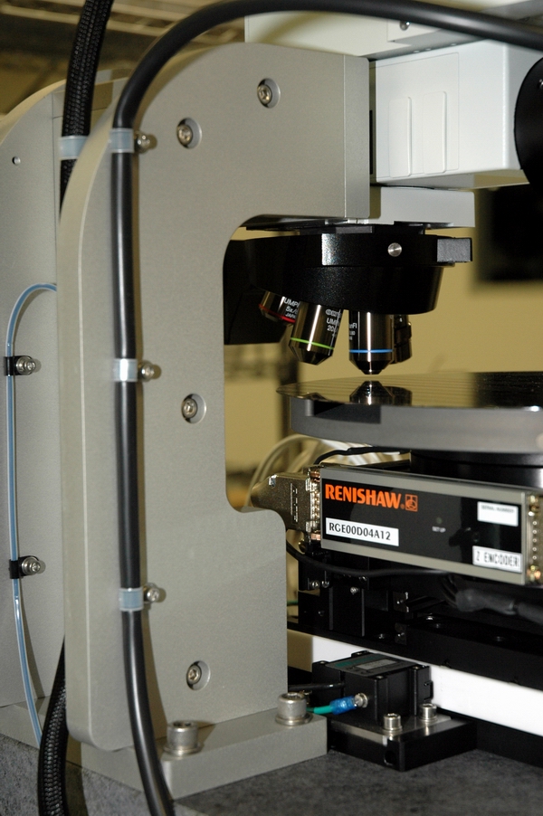
Developing a defect review module to integrate to the macro defect inspection tool required seamlessly integrating two imaging technologies. The defect review module must match the very high throughput of the macro defect tool and yet provide high quality, high magnification images of the regions of interest.
The Solution
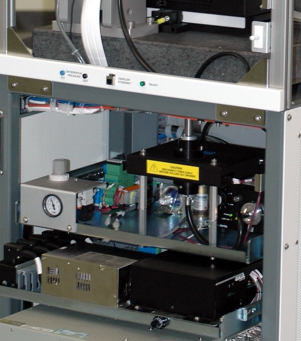
Owens Design’s first task was to create the system architecture for the review module which detailed the optical, software, and wafer staging requirements necessary to meet system performance measures. The optical system was refined through a set of image acquisition experiments and final selections for camera, objectives, and illumination were made. Vibration isolation design was critical as the module coupled directly to the macro defect tool. The software was developed in Microsoft .NET remote framework making integration with the host tool’s software robust.


