Semiconductor Equipment Development
Founded in 1983 and located in Silicon Valley, Owens Design has become synonymous with complex, custom development of semiconductor equipment.
Owens Design will accelerate your next-generation technologies from lab-to-fab, with prototype design to volume manufacturing – for inspection and metrology tools as well as wafer processing and handling systems.
Starting with hard disk drive manufacturing equipment designed and built over 40 years ago, Owens Design has successfully delivered over 65 product lines and 867 shipped systems to all major semiconductor fabs around the world with a record of 100% delivery. Our team of highly skilled engineers design and build prototypes based on a proven process that accelerates and scales your product development and manufacturing operations, efficiently while minimizing risk.
OEM New Product Development
Transform your IP into production-ready prototypes on accelerated schedules with the lowest risk possible
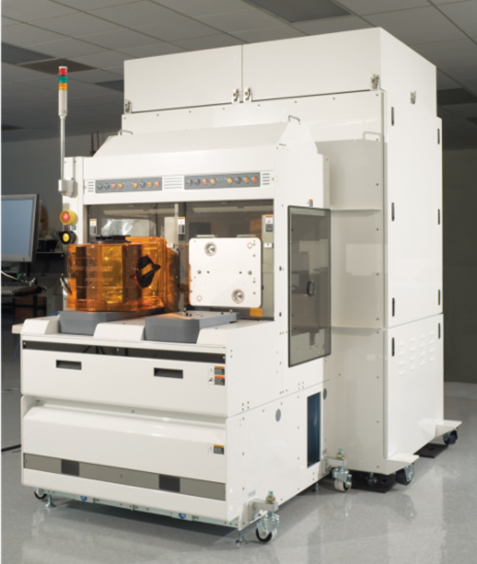
Factory Automation
Streamline complex manual processes and rapidly scale production with custom factory automation solutions
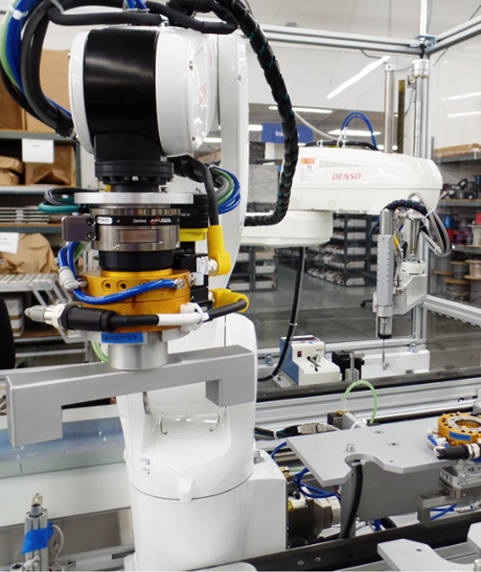
Design-to-Print Manufacturing
Outsource your manufacturing to an experienced partner that can also make design enhancements
Semiconductor Equipment Development Case Studies
Case Study: UV Chamber Design & Manufacturing for Flexible OLED Printing
Read moreA Precise, Custom Solution for Spin Coating Wafers on Film Frames
Read moreSemiconductor X-Ray Inspection Tool: From Prototype to Production without Alpha & Beta
Read moreMicro-Transfer Printing Tool Integration Brings Photonics Display Components to Life
Read moreSemiconductor Equipment Development Process
At Owens Design, we start with an exploratory process that differentiates us from other equipment development providers. Semiconductor equipment product development can be very expensive, so we have developed a phased development process to help our customers determine the best approach and architect a cost-effective solution.
This multi-phased process minimizes roadblocks later on in the development process.
Develop a Cost-Free ROM*
Owens Design estimates the cost to design and build the prototype along with cost for production systems as part of what we call Phase 0.
*Rough order of magnitude cost (+/- 25%)

Phase 1
If this fits your needs, Owens Design will proceed to Phase 1, which is a 4-6 week, in-depth collaborative process between you and Owens Design. This phase helps to reduce risk and accelerate the development cycle by establishing clear goals and specifications and selecting the overall architecture.

Tool Development
In Phase 2, we will proceed with design and build of your production-ready prototype.

Volume Manufacturing
Phase 3 is volume production with continuous improvement over time including BOM cost reductions. We can also assist with the transfer to your contract manufacturer, if your strategy calls for it.
Semiconductor Equipment Development Experience
We deliver product designs, prototype builds, CIP, customer specials and volume manufacturing services for the semiconductor and display original capital equipment (OEM) industries.
Metrology and inspection equipment is an Owens Design specialty:
- Delivery of 65 product lines and 867 shipped systems
- Reorders range between 4 to 234 units
- Two start-ups acquired by Tier 1 manufacturers
- Longest customer relationship is 15 years
Additional expertise:
- Front-end vacuum process equipment such as etch and deposition
- Back-end equipment including bonding, cleaning, testing, and wafer-level-packaging
- Atmospheric processing tools such as wet clean and printing
- Laser process development
- Semiconductor storage and buffer automation
Application Capabilities
- Substrate Handling: thick, thin and bonded wafer pairs, backside, edge and non-contact wafer handling
- Carrier Handling: film frames, dies and die trays, FOUPs, SMIF pods, cassettes, multiple generations of display glass, and flexible roll-to-roll web
- Controlled Environments
- Pressure regimes from atmospheric to ultra-high vacuum (<10-9torr)
- Thermal, vibration, humidity, O2, N2, B-field, light tight management
- Contamination: ISO Class 1, ISO 2 with mechanisms
- Precision alignment, staging, motion control micron-level repeatability
- Standards compliance, EFEM & SECS/GEM integration
- Full systems testing, drop ship directly to fabs
- Submicron wafer handling accuracy/precision
- Standards compliance S2, S8 and CE
- Production qualified by end users all over the world, including the world’s largest fabs in the USA, Korea, Taiwan, Europe, and China
- Trusted by fabs for next generation product testing
